Photon Crystal Energy Secures RMB 30 Million Angel Round, Using a Proprietary Ink Formula to Solve Scale-Up Challenges in Perovskite PV Module Manufacturing
This article reports Photon Crystal Energy's RMB 30 million angel financing round. Photon Crystal Energy focuses on the R&D and manufacturing of perovskite PV modules. The company has achieved more than 20% efficiency on 20 cm x 20 cm perovskite modules and has built a 10 MW pilot line for 30 cm x 30 cm modules, targeting 20% efficiency. The article also introduces the advantages of perovskite PV cells, including high theoretical conversion efficiency and low cost, as well as Photon Crystal Energy's innovations and technical breakthroughs in large-area manufacturing.
Photon Crystal Energy has achieved more than 20% efficiency on 20 cm x 20 cm perovskite modules. The company has also built a 10 MW pilot line for 30 cm x 30 cm modules, targeting 20% efficiency and aiming to set a new world record.
By Zhang Yichi
Edited by Su Jianxun
36Kr Carbon has learned that perovskite module company Photon Crystal Energy has completed a RMB 30 million angel financing round. The round was led by Zhengxuan Investment, with participation from Sinovation Ventures and Dingxiang Capital. The company has achieved more than 20% efficiency on 20 cm x 20 cm perovskite modules and has built a 10 MW pilot line for 30 cm x 30 cm modules, targeting 20% efficiency.
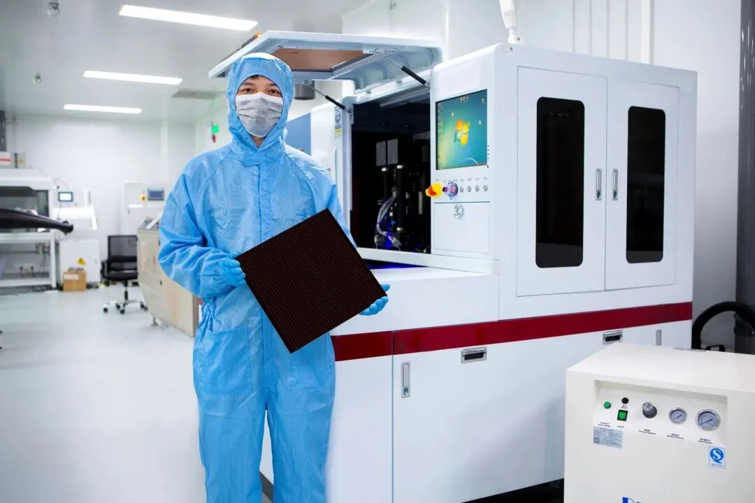
Photon Crystal Energy has produced 30 cm x 30 cm perovskite module samples.
The photovoltaic industry has evolved from first-generation crystalline silicon PV cells to second-generation thin-film PV cells, and now to third-generation PV cells represented by perovskites. Perovskite PV cells offer advantages such as high theoretical conversion efficiency, low material and production costs, strong low-light performance, and the potential for flexible manufacturing.
After years of development, crystalline silicon PV cells currently account for about 90% of the market. Although perovskite PV cells still face short-term technical challenges such as difficult large-area manufacturing and comparatively weaker stability, successful breakthroughs could give them strong potential to replace crystalline silicon PV cells.
Traditional crystalline silicon PV module manufacturing requires four factories. The first extracts metallurgical silicon from silica sand and produces high-purity silicon through refining and reduction. The second pulls the high-purity silicon into perfectly crystallized silicon ingots and cuts wafers with diamond wire. The next factory processes wafers into cells through cleaning, diffusion, coating, screen printing, and other steps. Finally, the cells and auxiliary materials are assembled into modules.
Compared with crystalline silicon PV modules, perovskite PV modules use inexpensive and readily available bulk chemicals as raw materials. The process flow is short, requiring only coating, laser scribing, encapsulation, and a few other steps, and the entire manufacturing process can be completed in a single factory. The investment cost per GW is about half that of crystalline silicon modules, while energy consumption per watt is only 0.12 kWh, one-tenth that of crystalline silicon modules. Therefore, once perovskite modules reach scaled production, they will have a significant cost advantage.
Photon Crystal Energy's core team was among the first groups of researchers to study perovskite industrialization and has deep experience in commercialization technology. CEO Huang Fuzhi serves as director of the Advanced Thin-Film Photovoltaics Research Center at the State Key Laboratory of Advanced Technology for Materials Synthesis and Processing at Wuhan University of Technology. He has published more than 150 papers in leading journals such as Science and Nature, with more than 10,000 citations. Since returning to China in 2015, Huang has focused on perovskite cell industrialization technology, developing a proprietary perovskite ink printing technology and publishing a Science paper as the sole corresponding author.
Huang told 36Kr Carbon that solving the challenges of large-scale industrialization for perovskite PV modules depends on balancing three factors: power conversion efficiency (PCE), area, and stability.

Relationship among power conversion efficiency (PCE), area, and stability.
In terms of efficiency, perovskite cells have already made a qualitative leap at the scientific level, and PCE is no longer the primary bottleneck for industrialization. In just about a decade, laboratory PCE for tandem perovskite cells has reached 31.3%, while laboratory PCE for single-junction perovskite cells has reached 25.7%. By comparison, it took nearly 40 years for mainstream crystalline silicon cells to reach 26% PCE. The theoretical PCE limit for crystalline silicon cells is 29.43%, leaving limited room for further improvement.
On why Photon Crystal Energy is prioritizing the industrialization of single-junction perovskite modules rather than higher-PCE tandem perovskite modules, Huang explained to 36Kr Carbon that although tandem perovskite cells have higher laboratory PCE, the technology requires covering crystalline silicon cells or another perovskite cell layer with perovskite material, which increases industrialization risk exponentially. Single-junction perovskite technology is the foundational technology for perovskite PV. Only after single-junction technology is solved can the industry move toward tandem, flexible, and other application directions.
The industrialization risks of tandem perovskite modules stem from the fact that the overall perovskite cell industrialization pathway is not yet mature. For a period of time, product stability may be relatively low and lifecycle relatively short. Taking two-terminal perovskite-silicon tandem modules as an example, if the perovskite layer fails earlier than the crystalline silicon layer, the entire module fails. For perovskite-perovskite tandems, Sn2+, Br-, and other elements must be introduced into the two perovskite layers to tune light absorption. These materials are less stable than conventional perovskite materials, and the process requires preparing two perovskite films, making large-area manufacturing even more challenging in terms of process and equipment. Therefore, industrializing single-junction perovskite modules is Photon Crystal Energy's current focus.
In large-area manufacturing, perovskite crystals tend to grow disorderly during drying after perovskite ink coating, and the larger the coating area, the harder this becomes to control. Disordered perovskite crystal films can easily form many pinholes, causing a significant drop in module PCE due to leakage. Improving large-area perovskite module manufacturing is therefore a key issue for the current stage of perovskite PV industrialization.
Although laboratory PCE for perovskite cells currently exceeds 25%, laboratory devices are made using spin coating. Spin coating can create uniformly distributed perovskite crystals and therefore higher PCE, but the forming area is very small, generally less than 1 square centimeter, and material utilization is only 3%, making it unsuitable for large-scale production.
Larger-area perovskite PV modules are generally made using slot-die coating, but module PCE is significantly affected as the area increases. Huang said that while perovskite cells can reach 25.7% under laboratory conditions, the industry is still working toward 16%-18% PCE for square-meter-scale perovskite modules. By comparison, large-area crystalline silicon modules can exceed 20% PCE. If mass-produced perovskite modules cannot improve PCE to above 18%, their levelized cost of electricity advantage will be greatly reduced despite their manufacturing cost advantage.
To reduce the impact of disordered perovskite crystal growth, Photon Crystal Energy has developed a proprietary perovskite ink formula. By tuning the perovskite ink, perovskite crystals do not form during coating. After a compact film is formed, dense perovskite crystals are generated through a reaction during annealing, avoiding the pain point of disordered crystal growth during drying. At the same time, the ink technology enables continuous slot-die coating and substantially improves production efficiency.
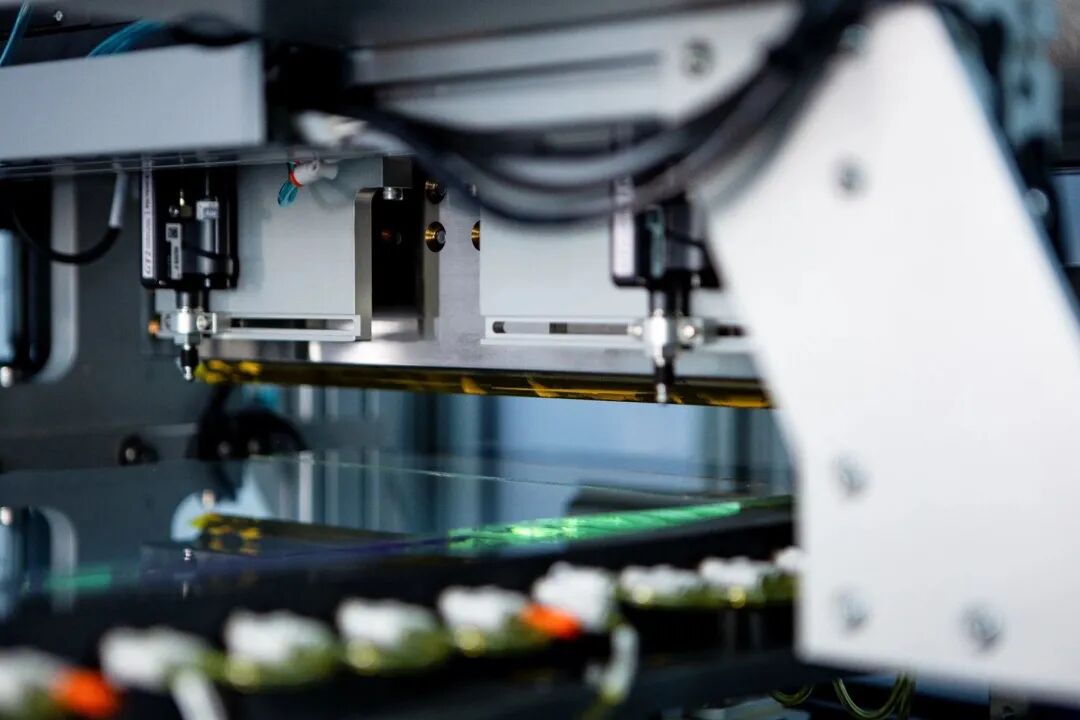
A high-precision slot-die coating machine used by Photon Crystal Energy, partial view.
In terms of stability, CTO Dr. Shi Lei first proposed the concept of improving perovskite cell stability through a sealed environment, developed full encapsulation technology for perovskite cells, set a stability record for perovskite cells, and published a Science paper as first author and corresponding author. Encapsulated cells can exceed the IEC 61215 test requirements for PV cells by several times. For example, they can withstand damp heat "double 85" testing for more than 1,800 hours with almost no degradation.
Photon Crystal Energy's team has extensive R&D experience in the PV industry. Chief Advisor Academician Cheng Yibing is a renowned scientist in the perovskite field, with more than 24,000 citations and 13 papers published in Nature, Science, and Nature family journals. On industrial manufacturing, Manufacturing Vice President Dr. Yao Guoxiao has rich experience in the PV industry. He previously served as CTO of NYSE-listed Yingli and as director and CTO of JinkoSolar, and is responsible for guiding Photon Crystal Energy's technology industrialization plan.
Photon Crystal Energy plans to build a 100 MW pilot line for 60 cm x 120 cm modules in 2023 and aims to achieve mass production on the 100 MW line in 2024.
Key Facts
- RMB 30 million
- IEC 61215
- 100 MW