Photon Crystal Energy: Printing Solar Energy Into Reality
Photon Crystal Energy follows a distinctive fully slot-die coating process to manufacture perovskite PV modules. Compared with mainstream vacuum processes, this route offers significant cost advantages and scale-up potential. With strong low-light power generation, broad temperature adaptability, and customizable color and transmittance, its products show strong potential in differentiated application scenarios such as BIPV, and the company is steadily advancing industrialization through demonstration projects.
On the Cover
This article is excerpted from the October 2025 issue of Pujiang Technology Review. Author: Research Team of Shanghai Science and Technology Innovation Finance Institute.
Cover | Case Study
Photon Crystal Energy: Printing Solar Energy Into Reality
As one of the most promising next-generation photovoltaic technologies, perovskite is moving from the laboratory to the industrial stage. To unlock large-scale commercialization at lower cost, Photon Crystal Energy has chosen a distinctive and difficult technical path, becoming the only perovskite module manufacturer in the industry that insists on using fully wet-process slot-die coating production technology.
As the world accelerates toward zero carbon, solar energy is shifting from a "clean promise" to the main engine of incremental energy growth. Photovoltaics directly convert sunlight into electricity and are taking on the core task of reshaping the energy structure. Against this backdrop, perovskite, one of the most promising next-generation PV technologies, is rapidly moving from the laboratory to the industrial stage.
Perovskite solar cells can match crystalline silicon PV in laboratory efficiency, while offering more significant advantages in cost and process. In addition, perovskite PV has excellent low-light performance and tunable optoelectronic properties, characteristics that crystalline silicon PV does not have. This gives perovskite PV greater imagination in application scenarios.
However, global perovskite capacity is still below 1 GW, and the entire industry remains in the critical incubation stage of moving from zero to one. It must overcome multiple barriers in technology, process, and market development. What path should the industry take? Pujiang Technology Review interviewed Photon Crystal Energy founder Huang Fuzhi to understand the company's distinctive route.
Manufacturing Perovskite Modules Through "Fully Printed" Technology
Photon Crystal Energy founder Professor Huang Fuzhi has worked for many years in materials science and third-generation printable solar cells. From academia to industry, he has personally witnessed and promoted the development of perovskite technology from fingernail-sized laboratory samples to scaled modules on a 100 MW pilot line.
Huang formulates functional materials into special "inks" and uses precision coating equipment to "print" them uniformly layer by layer onto a substrate, forming modules much like newspapers are printed. This method is called the "fully printed solution process," or "wet process." It has been Photon Crystal Energy's technical route since its founding and is one of the company's technical highlights.
This method is not mainstream in the industry.
At present, most manufacturers in the industry use the "vacuum dry process," a mature process borrowed from the semiconductor and traditional PV industries, with established equipment and workflows. Huang's reason for choosing "fully printed" technology is clear: to realize the true low-cost potential of perovskite technology.
The essential difference between the two routes is that the vacuum process requires operation in a vacuum environment. Equipment is expensive, energy consumption is high, and materials are lost during deposition, making it difficult for utilization to exceed 50%. Because the process is mature, the price of vacuum equipment is largely fixed, leaving little room for future cost reduction.
The printing process is entirely different. Materials are coated directly in liquid form, and utilization is close to 100%. The equipment is relatively simple and has already been fully localized in China, leaving significant room for cost reduction. More importantly, the printing process is fast and has strong scale-up potential. In the future, when expanding from 100 MW to GW scale, the vacuum process would require linearly adding large amounts of expensive equipment, while the printing process may only need larger coating areas and faster speeds, allowing a small number of production lines to meet capacity needs.
"It has very large room for future cost reduction. That is why we chose this technical route," Huang said. "But we also chose the hardest road." The word "hard" runs almost through Huang's entire journey from academic research to industrialization. From entering the perovskite field as a researcher in Australia in 2013, to returning to China in 2015 to teach at Wuhan University of Technology, Huang built a team and focused its research on perovskite industrialization.
In the laboratory, perovskite cells are only the size of a fingernail. They can be made precisely and uniformly, with high efficiency. Once scaled up, even to 5 cm x 5 cm, defects multiply and efficiency drops sharply. "The larger the area, the higher the requirements for film quality," Huang explained. The team's core task was to solve the "damage-free scale-up technology" for perovskites: increasing area tenfold or a hundredfold while keeping the number of film defects basically unchanged.
After years of effort, the team solved this challenge in 2021 and published the results in the international top journal Science. The paper demonstrated the efficiency and stability of scalable solution-process devices over larger areas, providing evidence for engineering implementation. With this key technology breakthrough, Huang founded Photon Crystal Energy in 2022 and officially advanced the technology, refined in the laboratory for nearly a decade, toward industrialization.
In August 2024, Photon Crystal Energy's 100 MW perovskite pilot line in Foshan, Guangdong, was commissioned. It is currently the world's only 100 MW production line using a proprietary ink formula and fully printed technology. The line has already achieved small-batch shipments, producing 1.2 m x 0.6 m modules with photoelectric conversion efficiency above 18%, combining high efficiency with low cost. This pilot line carries the team's vision and represents a key step toward truly realizing industrial-scale production and commercialization of perovskite technology.

How to Challenge Mature Crystalline Silicon
Photon Crystal Energy's 18% module efficiency is a solid starting point in the early stage of industrialization. But one unavoidable question remains: when mainstream crystalline silicon module efficiency on the market has generally reached 23% or 24%, where is perovskite's competitiveness?
This is not a simple numerical comparison. In fact, to truly evaluate the merits of a PV technology, laboratory standard efficiency, real-world power generation performance, and final application scenarios must all be considered. This is the logical starting point for perovskite's challenge to mature crystalline silicon.
First, in terms of power generation, the key is total lifecycle electricity generation, not a single peak efficiency number.
"You cannot only look at the highest efficiency point in the laboratory," Huang explained. "You have to look at how much electricity it can generate across the entire lifecycle in real environments."
Perovskite has two major characteristics that give it potential advantages in total power generation.
The first is excellent low-light performance. Sunlight is not constant. Under low-light conditions such as mornings, evenings, and rainy days, perovskite can still maintain relatively high power generation efficiency, while crystalline silicon efficiency drops significantly. This means perovskite has longer effective power generation time each day.
The second is a wider operating temperature range. PV modules heat up under sunlight, and the higher the temperature, the lower the power generation efficiency. Crystalline silicon modules show clear efficiency degradation at high temperatures, while perovskite is much less affected by temperature. "Simply put, the hotter the summer, the more obvious our advantage becomes," Huang said.
Based on these two points, he proposed a conclusion: "According to our calculations, a perovskite module with 22% conversion efficiency can generate enough electricity over a full year to match a crystalline silicon module with 24% efficiency." This conclusion provides the core value support for perovskite while its efficiency number still temporarily lags behind.
Second, in terms of applications, perovskite creates a leap in value by opening new scenarios that crystalline silicon cannot cover. The most promising of these is BIPV, or building-integrated photovoltaics.
Under the dual-carbon goals, energy conservation and emission reduction in buildings are top priorities. Achieving carbon neutrality means not only reducing emissions, but also offsetting traditional energy consumption through new energy. Among all forms of new energy, only photovoltaics can be perfectly integrated into buildings themselves. However, traditional crystalline silicon PV has always faced a core barrier in building applications: aesthetics.
"Buildings have consumer attributes. They are connected to people, and people pursue aesthetics. If it does not look good, people will not want it," Huang said, pointing directly to the issue. Crystalline silicon modules have a single color and are completely opaque. If they replace glass curtain walls, people would have to stay in "dark rooms," which is not feasible in practice.
Perovskite changes this completely. By adjusting formulas and processes, it can be made into semi-transparent "power-generating glass" in different colors. "You can choose different levels of transmittance. It can replace all building glass. Future glass curtain walls and skylights will themselves be power-generating building materials." For building facades, opaque perovskite modules can also be tuned into rich colors to match the aesthetic design of the building. This effectively gives architects a new "design element" with power generation capability.

BIPV building curtain wall. Image source: Photon Crystal Energy.
Therefore, in BIPV, the core of competition is no longer simply the cost of electricity generation, but the integration of aesthetics, transmittance, power generation function, and architectural design. As national requirements for PV application ratios in new buildings become higher, this development path is inevitable.
In addition, perovskite's light, thin, and flexible characteristics allow it to enter scenarios such as outdoor tents and wearable devices, creating new demand. Outside the enormous shadow of crystalline silicon, opening a differentiated development path of its own is where next-generation PV technology has the opportunity to achieve truly disruptive innovation.
Crossing the Early Industrial Chasm
Although perovskite technology has enormous potential, it faces a crystalline silicon PV industry that has developed for more than 30 years and has a highly mature industrial chain. In recent years especially, overcapacity in crystalline silicon has triggered fierce price wars and continuously driven down module costs, creating enormous real-world pressure for the newly emerging perovskite industry.
This is a typical issue in the iteration path of emerging technology industries. Facing mature dominant products, latecomers may have obvious advantages, but still need to open market gaps step by step and find their foundation.
In Huang's view, perovskite industrialization will not be a rapid disruption. The new industrial chain needs patient cultivation. This is not only one company's exploration, but also a reflection of how an emerging industry can find a solid path for survival and development in front of mature crystalline silicon.
First, in the early stage of industrialization, the core task is to find a foothold through differentiated applications. Directly competing with crystalline silicon on cost in the mainstream utility-scale ground power station market is clearly unrealistic. Therefore, the only way forward is to find niche markets that crystalline silicon technology cannot meet, or cannot meet well enough.
The key to entering these markets is building customer trust. Huang said frankly that the biggest obstacle for new technology is market skepticism. Due to the lack of long-term outdoor operating data and complete industry standards, early commercial customers are generally cautious. Therefore, accumulating real data through demonstration projects and verifying product reliability across the three core indicators of efficiency, area, and stability are the top priorities at this stage.
Second, scaled production is needed to achieve cost competitiveness. Huang has a clear forecast: when industry scale grows from the 100 MW level to the GW level, the production cost of perovskite modules is expected to fall from more than RMB 1 per watt today to about RMB 0.8 per watt. When scale further expands to the 10 GW level, cost will fall below RMB 0.6 per watt. If this cost level is achieved, perovskite products will be able to compete directly with crystalline silicon in mainstream markets such as large ground-mounted power stations.
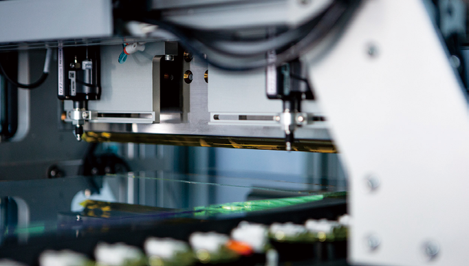
Slot-die coating printer. Image source: Photon Crystal Energy.
Behind cost reduction is the maturation of the entire industrial chain: standardized production equipment and substantially amortized depreciation; stable supply chains for core materials and lower procurement costs; continuous optimization of production processes; and ongoing improvements in yield and efficiency, gradually shaking the existing PV landscape.
During this process, there is also a somewhat compromising technical route: perovskite-silicon tandem cells. This is not a simple replacement relationship, but rather a possibility for "collaboration" at the current stage. By stacking perovskite films on mature crystalline silicon cells, cell efficiency ceilings can be raised above 30%. This provides an upgrade direction for the crystalline silicon industry facing efficiency bottlenecks and also gives perovskite technology a way to integrate into the existing massive industrial system.
However, Huang emphasized: "Single-junction is the core; tandem is the future." In his view, only after single-junction perovskite's own cost, efficiency, and stability are fully validated by the market will large-scale application of tandem technology become truly natural.
From the laboratory to the production line, Huang Fuzhi and his team have spent more than a decade beginning the road to industrialization. They started by looking for a foothold in edge markets, then gradually moved toward the mainstream by building trust and expanding scale, exploring the future of photovoltaics. This is a miniature of the zero-carbon energy revolution, a journey that tests patience, with a destination that is a bright future powered by light.
Key Facts
- Fully wet-process printing